 For a while now I’ve been dying to share some of the new nanostructures I’ve discovered during ion-assisted vapor deposition of CI(G)S thin films. My paper was published in the Journal of Applied Physics last fall (sorry for the blog outage over the winter-break). The paper is titled: “Nanostructured light-absorbing crystalline CuIn(1–x)GaxSe2 thin films grown through high flux, low energy ion irradiation;” http://dx.doi.org/10.1063/1.4823987. There are a lot of unanswered questions about the work that leaves me dreaming up different solutions to how these films are growing. I discovered three major growth conditions altered by the ionized gas in our growth chamber. One was a high-aspect ratio platelet (so thin as to be electron transparent- making for very easy TEM sample preparation).
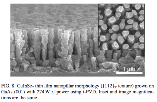
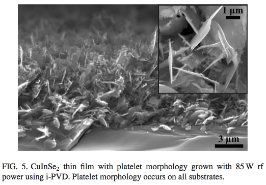 The platelets were crystalline CIGS with facets on the {112} planes as expected. A middle region (in terms of growth temperature) which exhibited a transition between platelets and other structures in the film. Essentially an influenced/broken epitaxial growth on GaAs substrates but with large areas of void and vertical and lateral growth causing over-hangs in the film. And finally a wonderful structure seen in the figure above (Fig.8 from my paper) – a nanopillar forest of CIGS crystalline thin films that appear to be somehow registered to the GaAs substrate. Normally I would expect epitaxy at these temperatures (720°C+). However, the substrate used was p-(001) GaAs wafer and the nanopillar film was found to be textured on the {112} tetragonal plane. Quite interesting! I believe this to be solely due to the high-flux low-energy ion-bombardment caused by the rf-plasma coil.
The high aspect ratio nanopillars and platelets are black to the eye and absorb a wide-band of light at a large number of angles of incidence, making them highly absorbing structures possibly useful for light-trapping solar-cells. I find that possibility exciting, especially in the flat-topped nanopillars, which may afford new ways of heterojunction partnering.
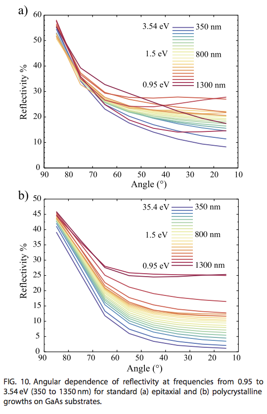
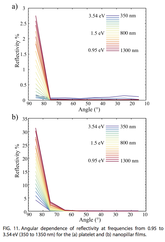 Incidentally, JAP editorial staff accidentally reversed two figures, so I’m publishing an erratta here on my blog. The two figures should be recognized as being clearly out of place based upon the text of the article as well as the abstract. I missed it in the author-preview, so I cannot fault the editorial staff for something I missed in pre-publication. Even though this was caught before publication the change required a separate erratum to be published, which I felt was perhaps un-necessary due to the glaring error. So, in the article as published, please note that the figure caption and figure numbers for figures 10 and 11 are swapped. One figure shows the angle-resolved reflectivity of the polycrystalline and epitaxial standard growths, while the other figure shows the same for the nanostructured films. Of course we expected (as disclosed) that the nanostructured films (much like the moth-eye structure) are more light-trapping than the standard film growths, and therefore the reader can easily see the two figures are incorrect. If you’d like to read my article in full, please feel free to download it here.
I have been working on extensions related to this work that I wish I could discuss here, but can’t until the work is finally disclosed. I do feel that this type of technology may pave the way for more advanced thin film PV devices, however, this type of advanced structure needs to arise from simple deposition methods that are scalable to industrial size-scales. What is wonderful is everything used in this deposition is scaleable to industrial sizes. So these structures are quite interesting to consider for large-scale production.